Lab-14 MOSFET
Objectives
This lab will introduce you to MOSFETs (metal-oxide-semiconductor field effect transistors). You will build a MOSFET inverter and determine the voltage transfer characteristic of this device (\(V_{out}\) vs. \(V_{in}\)). From this transfer characteristic you will learn how to extract information about the MOSFET such as threshold voltage (\(V_T\)).
In the cutoff and linear regions the MOSFET approximates the operation of a switch. In between these two regions lies the saturation region. In saturation the MOSFET makes a good amplifier.
Components Required:
One CD4007
One 10K ohm resistor
One Breadboard
One Bag of wires
Four pairs of banana to alligator
Note: The lab measurements can be done as a group. However, the plots should be done individually. All results should be submitted to Blackboard individually.
MOSFET characteristics:
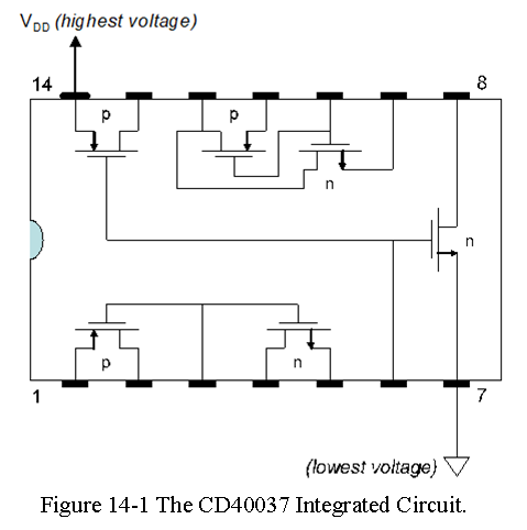
The MOSFETs that you will be using for this lab are in a 14-pin package as shown in Figure 14-1. Study this diagram and become familiar with the layout of the individual MOSFETs within the CD4007 chip. Notice there are three n-channel devices and three p-channel devices. Although some devices share pins, all terminals for each device are available at an external pin on the chip.
MOSFETs are actually 4-terminal devices: gate, drain, source, and substrate. In the CD4007 the substrates for all n-channel devices are connected to pin 7. Likewise, the substrates for all p-channel devices are connected to pin 14. For proper function of the MOSFETs you must attach pin 7 to the lowest potential in your circuit (usually ground) and you must attach pin 14 to the highest potential in your circuit (\(V_{DD}\)).
MOSFETs are susceptible to electrostatic discharge (ESD). You have no doubt experienced large ESDs if you have ever scuffed your feet across a carpet and touched a metallic object. Even very small ESDs can damage a MOSFET by blowing-out the gate oxide. This is mainly because the gate oxide is very thin (<< 100 nm). These MOSFETs have been protected from minor forms of ESD by two clamping diodes attached to each gate. One diode prevents \(V_{GS}\) from exceeding \(V_{DD}\) (pin 14) + 0.7 V. The other prevents \(V_{GS}\) from becoming more negative than \(V_{SS}\) ( pin 7) - 0.7 V.
Concept: The DC voltage transfer characteristic of a MOSFET inverter
Build the simple MOSFET inverter shown in Figure 14-2. Use the rightmost MOSFET in the chip: gate connected to pin 6, source to pin 7, drain to pin 8. Don’t forget to connect pins 7 and 14 as described above!
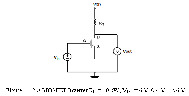
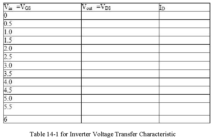
- Measure the voltage transfer characteristic for the MOSFET inverter by varying \(V_{in}\). Use the table below to guide you in selecting the appropriate data points.
Notice that the circuit is an inverter: when the input voltage is “high,” the output voltage is “low” and vice versa.
- When the gate reaches the threshold voltage, the MOSFET begins to conduct current through the drain (\(I_D\)) and starts to invert. Based on the measurements in part (a), what is the approximate Threshold voltage (\(V_T\)) for this MOSFET?
Plot the square-root of Drain current against Input voltage (\(V_{GS}\)) . The active region now becomes a straight line. Extrapolate this straight line to the Input voltage axis . The intercept gives us the accurate Threshold voltage \(V_T\).
Plot the voltage transfer characteristic (i.e., \(V_{out}\) vs. \(V_{in}\)) in your lab report. Identify the three regions of MOSFET operation on your plot:
Cut-off:\(V_{GS}~ \lt~ V_T\) Saturation:\(V_{GS}~ \gt~ V_T\) and \(V_{DS}~\gt~V_{GS}-V_T\) Linear: \(V_{GS}~gt~V_T\) and \(V_{DS} ~\lt~V_{GS}-V_T\)
- Submit all results into Blackboard Brightspace.