Lab-9 Diode Characterization:
Name: Write down your name
Date: Date of report submission and date of lab performed
Learning Objectives:
To reinforce the concepts on diode circuit analysis
- Verification of diode theory and operation
- To understand certain diode applications, such as rectification and clipping.
Diode Theory and Operation:
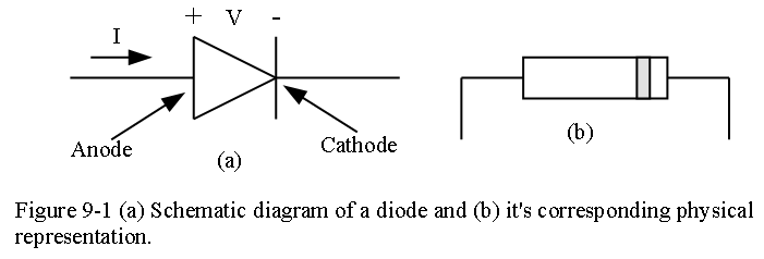
A solid state diode can be pn-junction diode) or a metal-semiconductor Schottky barrier diode. Regardless of the type, the circuit symbol for a diode is as shown in Figure 9-1(a) and the corresponding device symbol in Figure 9-1(b).
If V is positive, the diode is forward-biased and the diode can conduct a significant positive current I, even though V is a small voltage (typically 0.7 V for the most common [silicon] diodes). If V is negative, the diode is reverse-biased; the negative current produced by the reverse bias is so small that it is often considered to be zero. Thus, the usual function of a diode is to allow current to flow in the direction of the arrow (the forward direction) for positive V’s, but doesn’t allow any current to flow in the reverse direction for negative V’s.
Only a small forward bias (positive V) is required to cause a diode to conduct a significant current I, and the less this voltage, the better. One model of an ideally diode has the following properties:
This voltage drop for forward bias is zero volts. The diode can conduct any value of current I in the forward direction, with this value being determined not by the diode, but by other components in the circuit in which the diode is connected. The diode conducts zero amperes for a negative V, regardless of the voltage magnitude.
In other words, an ideal diode is a short circuit for a voltage V that tends to be positive (but it cannot be more than 0 V) and an ideal diode is an open circuit for a negative V. Thus, an ideal diode acts like a switch that is closed for current flow in the direction of the arrow in the diode circuit symbol, and open otherwise. Essentially, it is an electronically operated switch.
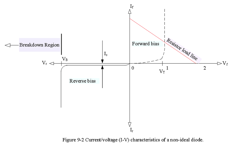
Figure 9-2 shows the I-V characteristic of an actual, physical diode. The part of the curve in the first quadrant is the forward characteristic, and the part in the third quadrant is the reverse characteristic. The current \(I_S\) is called the reverse saturation current. For a reverse voltage \(V_B\), the diode “breaks down” and draws a large reverse current.
The current through an ideal pn junction is given by the diode equation.
\[i_D(V) = I_s\left[exp\left(\frac{eV}{nkT}-1\right)\right]~~~~(9.1)\] where V is the voltage drop across the junction, \(I_s\) is a constant reverse saturation current and depends on the temperature, geometry of the junction, e is the electronic charge, \(e = 1.6\times 10^{-19}~C\) and \(k=1.38\times 10^{-23}~J/K\) is called Boltzmann’s constant and T is the temperature in Kelvin (K). The constant n varies from 1 to 2.
Nonlinear Circuit Equilibrium:
An electric circuit containing nonlinear elements like diodes cannot be reduced to systems of linear equations. Consequently, the equilibrium voltages and currents in nonlinear circuits are much more difficult to determine. Using Multisim these equilibrium quantities can be found, however approximate analysis methods are often useful, particularly for simple circuits. Two quick methods can be used: (i) Graphical Analysis and (ii) Iterative Analysis.
(i) Graphical Analysis – Load Lines:
Consider the simple circuit as shown in Figure 9-3 which contains a voltage source \(V_S\), a resistor R and a generic nonlinear component with impedance Z(V), where V is the voltage across the component. Regardless of behavior of the nonlinear component, the voltage source and resistor set certain constraints on the possible equilibrium voltages and currents. For instance, the current i cannot exceed \(V_S/R\), the current that flows when the impedance of the nonlinear component Z is zero. Under these conditions, the voltage V across the nonlinear component is zero. Alternately, V cannot exceed the voltage of the source \(V_S\), and this maximum voltage is only obtained when the impedance Z is infinite and \(i_D=0\). Impedances between zero and infinity produce intermediate values of the current and voltage. (We have assumed here that the nonlinear device does not contain any internal power source, hence Re(Z) ≥ 0.)
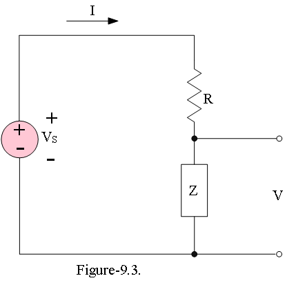
The possible values fall on a curve given by the parametric equations \(i_D=V_S/(R+Z)\) and \(V=ZV_S/(R+Z)\), where Z varies between zero and infinity. Eliminating Z demonstrates that the curve is actually a straight line given by the equation
\[i_D(V)=\frac{(V_0−V)}{R}~~~~(9.2)\]
This equation could have been derived directly from its end points, \(i_D=V_S/R\) at V=0 and \(i_D=0\) at \(V=V_S\). The line determined by Eq. (9.2) is called the load line because it is determined solely by the load (and the power source), not by the nonlinear component.
The nonlinear component obeys its own equation, or “characteristic” curve \(i_Z(V)\). In equilibrium, both the load line and the characteristic curve must be satisfied simultaneously. Consequently the equilibrium current and voltage for the circuit are given by the intersection of the load line (Eq. (9.2)) and the characteristic equation \(i_Z(V)\).
(ii) Iterative Analysis:
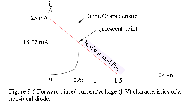
For example, a nonlinear device in the circuit shown in Figure 9.4 has the I-V characteristic given for for the following parameters:
\[V_S=V_{Th}=1.5 V, R=R_{eq}=60\Omega\]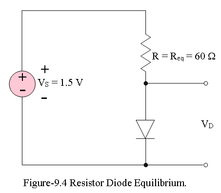
Determine the voltage across and the current through the nonlinear device. Using KVL we get,
\[V_S-i_D-V_D=0\] \[i_D=\frac{V_S-V_D}{R}=\frac{1.5V-V_D}{60}~~~~(9.3)\] \[i_D=\frac{1.5V-V_D}{60}=0~~if~~V_D=1.5V\] \[i_D=\frac{1.5V-0}{60}=25mA~~if~~V_D=0V\] An approximate diode current can be expressed as
\[i_D = I_se^{\alpha V_D}~~~~(9.4)\] Using Eq.(9.4) and using approximate data from Figure 9.4, we can determine the unknown parameter \(\alpha\).
\[1mA=I_se^{0.6\alpha}~~~~(9.5)\] \[30mA = I_se^{0.7\alpha}~~~~(9.6)\] Dividing Eq. (9.6) by Eq. (9.5) we get, \[30=e^{0.7\alpha-0.6\alpha}; 30 = e^{0.1\alpha}; \frac{ln30}{0.1}=\alpha; \alpha =34\] Now using the value of \(\alpha = 34\) and using Eq. (9.5) or Eq. (9.6), we can determine the reverse saturation current \(i_{sat}\) as follows:
\[1mA=I_se^{(0.6)(34)}; I_s=1.38\times 10^{-12}A\] Now using Eq. (9.4), we get
\[i_D = (1.38\times 10^{-12}A)e^{34V_D}\], hence \[V_D=\frac{1}{34}ln\frac{i_D}{1.38\times 10^{-12}A}~~~~(9.7)\] Now using Eq.(9.3) and Eq. (9.7) iteratively, we can generate the following table for first four iterations and are given in the Table 9.1. The results have converged to three decimal places.
\[i_D=\frac{V_S-V_D}{R}=\frac{1.5V-0.75}{60}=12.5mA\] \[V_D=\frac{1}{34}ln\frac{0.0125}{1.38\times 10^{-12}A}=67431mV\] \[i_D=\frac{V_S-V_D}{R}=\frac{1.5V-0.67431}{60}=13.7613mA\] \[V_D=\frac{1}{34}ln\frac{0.0137613}{1.38\times 10^{-12}A}=67715mV\] \[i_D=\frac{V_S-V_D}{R}=\frac{1.5V-0.67715}{60}=13.7142mA\] \[V_D=\frac{1}{34}ln\frac{0.0137159}{1.38\times 10^{-12}A}=67705mV\]Table 9-1 Iterative Process of Finding Diode Voltage(mV) and Diode Current (mA).
| Iteration | \(V_D(mV)\) | \(i_D(mA)\) |
|---|---|---|
| 1 | 750 | 12.5 |
| 2 | 67432 | 13.7613 |
| 3 | 67715 | 13.7142 |
| 4 | 67705 | 13.7159 |
| 5 | 67705 | 13.7159 |
Finally, plotting the data as generated in Table 9.1 is shown in Figure 9.5.