Lab-15 CMOS Inverter
Name: Write down your name
Date: Date of report submission and date of lab performed
Objective:
The objective of this experiment is to characterize a CMOS inverter in both loaded and unloaded conditions. By manipulating the board layout of the chip, we also hope to give further insight as to how the CMOS inverter operates.
Materials:
1 - CD4069 inverter chip
1– 10K ohm resistor
5 - 47 pF capacitor
1 - Bag of wires
1 – Breadboard
2 – pair of banana to alligator clips
2 – scope probes
NOTE This lab can be done as teams but reports must be submitted individually to Bb
Tasks:
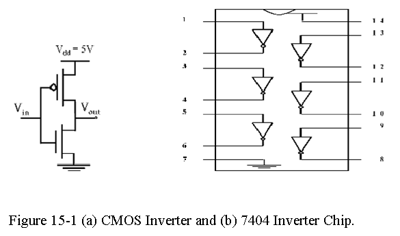
- Wire up the CMOS inverter shown in Figure 1 and characterize it.
In order to accomplish this -
Obtain a CD4069 inverter
Attach 5.0V to Vdd (pin 14) and ground (pin 7) to Gnd.
To find the VTC –
Attach a 2nd power supply output to the inverter input and the 2nd Gnd to Ground.
Begin at 0V and vary the input voltage by 0.25 V. Do not exceed 4.5V.
Draw the image below

- Now wire up a 10.0k resistor from Vdd to the gate output
- Draw the new VTC on the same graph as above. Be sure to label the new one.
- How does the extra resistor affect the VTC? Explain why this resistor affects it.
- To find the propagation delay –
- Wire up a ring oscillator using 5 CMOS gates as shown in Figure 15-3.
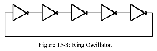
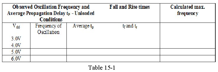
- Using the oscilloscope, measure its oscillation frequency at the supply voltages listed in the table below
- Measure the average propagation delay of a gate at each supply.
- Measure the fall and rise times.
- Calculate the maximum frequency from the measured rise and fall times
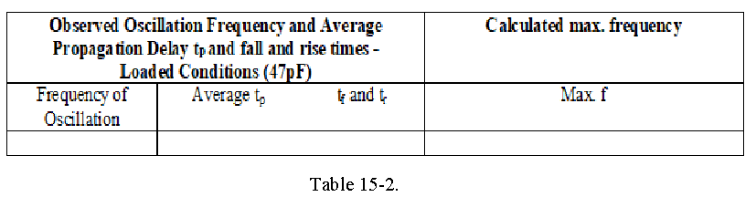
Now attach a 47.0 pF load capacitor from the output of each gate to GND and measure the oscillation frequency at \(V_{dd}\) = 5.0 V.
Repeat the steps above for loaded conditions and \(V_{dd}\) = 5.0 V.
Submit to Blackboard Brightspace.